Overview
Software: KiCad
Board Size: 80 mm × 40 mm
Author: Abel Paul John
Section 1: Task 1 – Manual LED Chaser (CD4017 + Push Button)

In the first task, I designed a manual LED chaser circuit using the CD4017 decade counter. The idea is simple: each time the push button is pressed, the counter advances to the next output and turns on the next LED.
To make the circuit stable, I added a debounce network using a resistor and a capacitor. This prevents unwanted multiple triggers caused by mechanical button bouncing. A pull-up resistor ensures that the clock input always has a defined logic level when the button is not pressed.
Each output of the CD4017 is connected to one LED through a current-limiting resistor. This protects the LEDs and guarantees uniform brightness.
The schematic design focused on correct pin connections, clean signal flow, and proper power distribution.
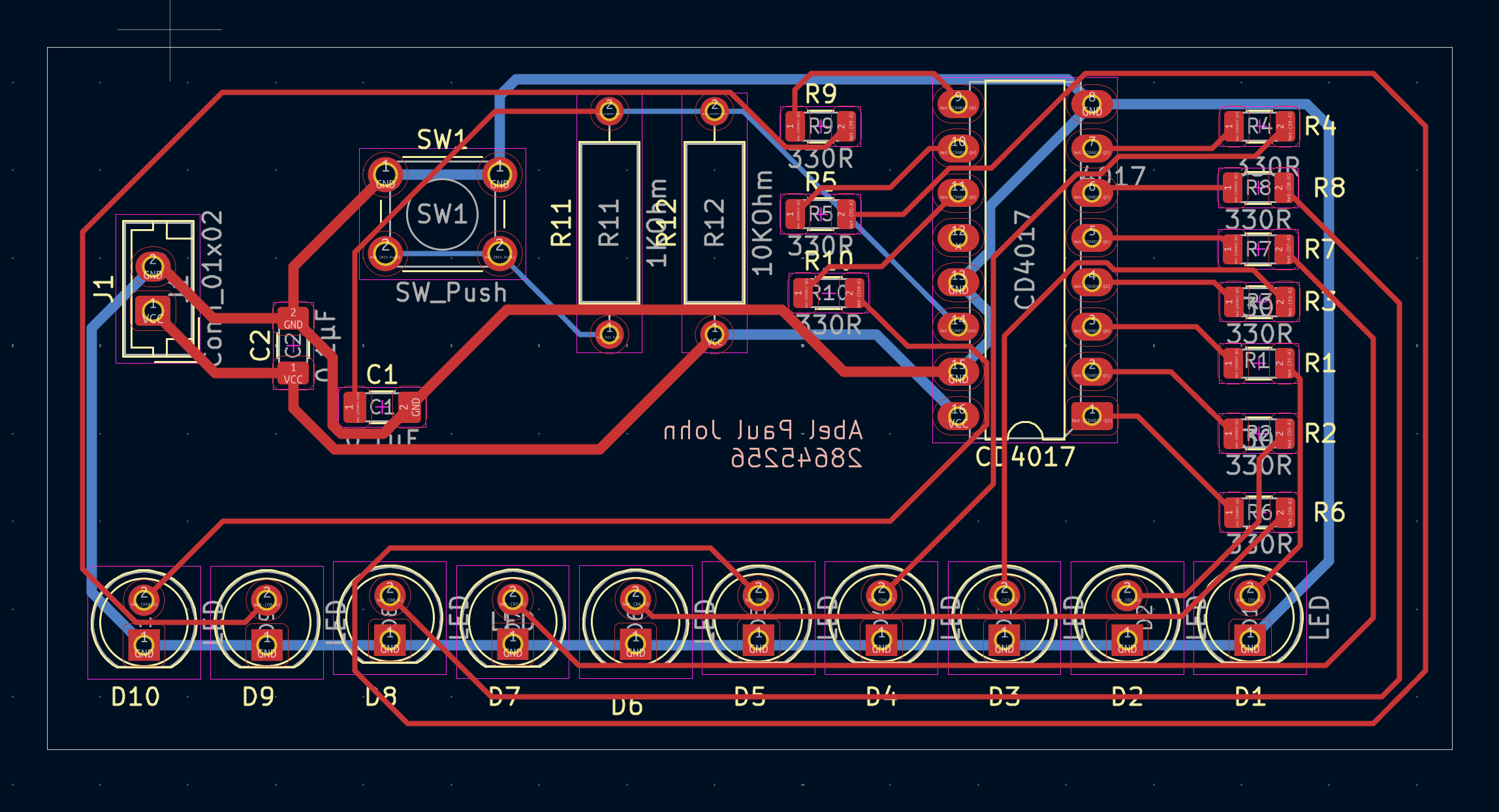
After completing the schematic, I moved to the PCB layout. The board size was fixed at 80 mm × 40 mm, and strict routing rules were applied. Only horizontal, vertical, and 45-degree traces were allowed. The number of vias was limited, so component placement had to be optimized carefully before routing.
I arranged the LEDs in a straight row to create a clean visual sequence. The CD4017 was placed close to the LED resistors to reduce trace length. Power and ground traces were made wider than signal traces to improve reliability.
The final routing is structured, readable, and easy to manufacture.

The 3D view confirms that all components are correctly aligned and properly spaced. The silkscreen labels are readable, and the LEDs are positioned in a clean linear arrangement.
This validation step ensures that the board is ready for fabrication and manual soldering.
Section 2: Task 2 – Automatic LED Chaser (NE555 + CD4017)
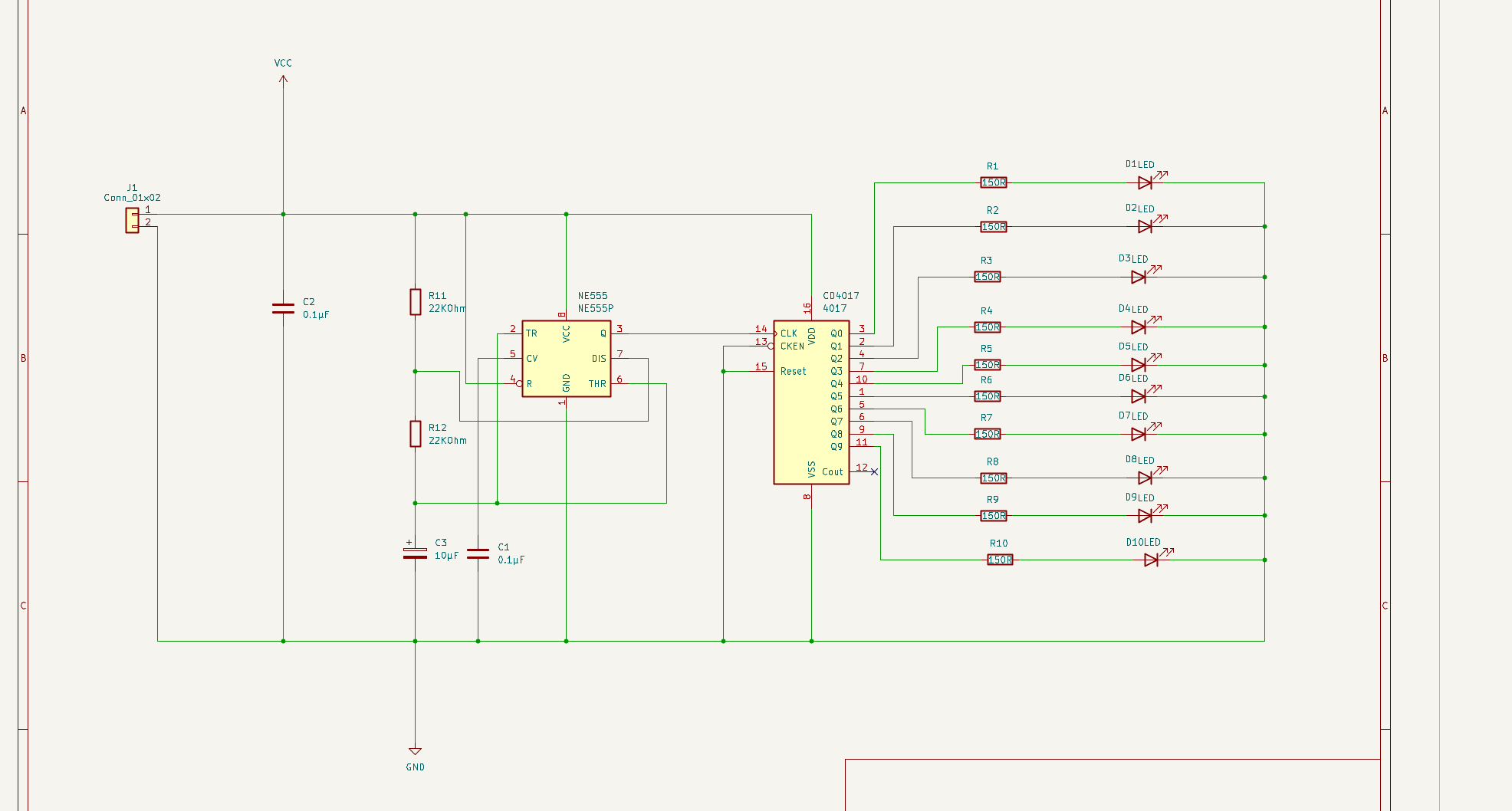
In the second task, I replaced the push button with an NE555 timer configured in astable mode. The goal was to generate a continuous clock signal so that the LEDs automatically move in sequence.
The NE555 produces a square wave at its output pin. This signal is connected to the clock input of the CD4017. I calculated the frequency using the astable timing formula and selected resistor values from the E12 series to achieve approximately 4 Hz. This frequency creates a smooth running light effect.
Additional bypass capacitors were placed near the IC supply pins to ensure stable operation.

The second PCB design is more complex because of the additional timer IC. I reorganized the placement to maintain logical signal flow from the NE555 to the CD4017.
The clock trace was kept short to reduce noise. Timing components were placed close to the NE555. Power routing was carefully managed to ensure stable voltage supply for both ICs.
Despite the added complexity, the board still follows all layout constraints, including limited vias and controlled routing angles.

The 3D rendering confirms correct component orientation and spacing. The LED row remains symmetrical, and both ICs are clearly positioned. The overall layout appears professional and production-ready.
Final Section: Engineering Approach & Learning Outcome
Through these two tasks, I demonstrated the complete workflow from schematic design to final PCB layout and 3D validation.
I applied structured engineering thinking: first understanding the functional requirements, then designing the circuit, optimizing component placement, defining net classes, routing signals carefully, and finally verifying the board in 3D.
The progression from a manual clock system to an automatic timer-based system shows both conceptual understanding and technical improvement.
This project reflects my skills in digital electronics, timer circuits, PCB layout discipline, and hardware development using KiCad.
End of Case Study.
View all projects