Precision Analog Design: Op-Amp Circuits in Falstad
Overview
In this project, I designed and simulated different analog circuits using operational amplifiers and resistor networks. The goal was to understand how small voltage differences can be measured, amplified, and converted into a stable output signal.
Before building the circuits on a real breadboard, I tested everything in simulation. This helped me check the voltage levels, current flow, gain behavior, and overall stability of the system. By doing this, I reduced the risk of errors and improved my understanding of analog electronics.
The project contains three main parts:
- A Wheatstone bridge with a differential amplifier
- A weighted operational amplifier circuit
- A voltage divider network with amplification
1. Wheatstone Bridge with Differential Amplifier
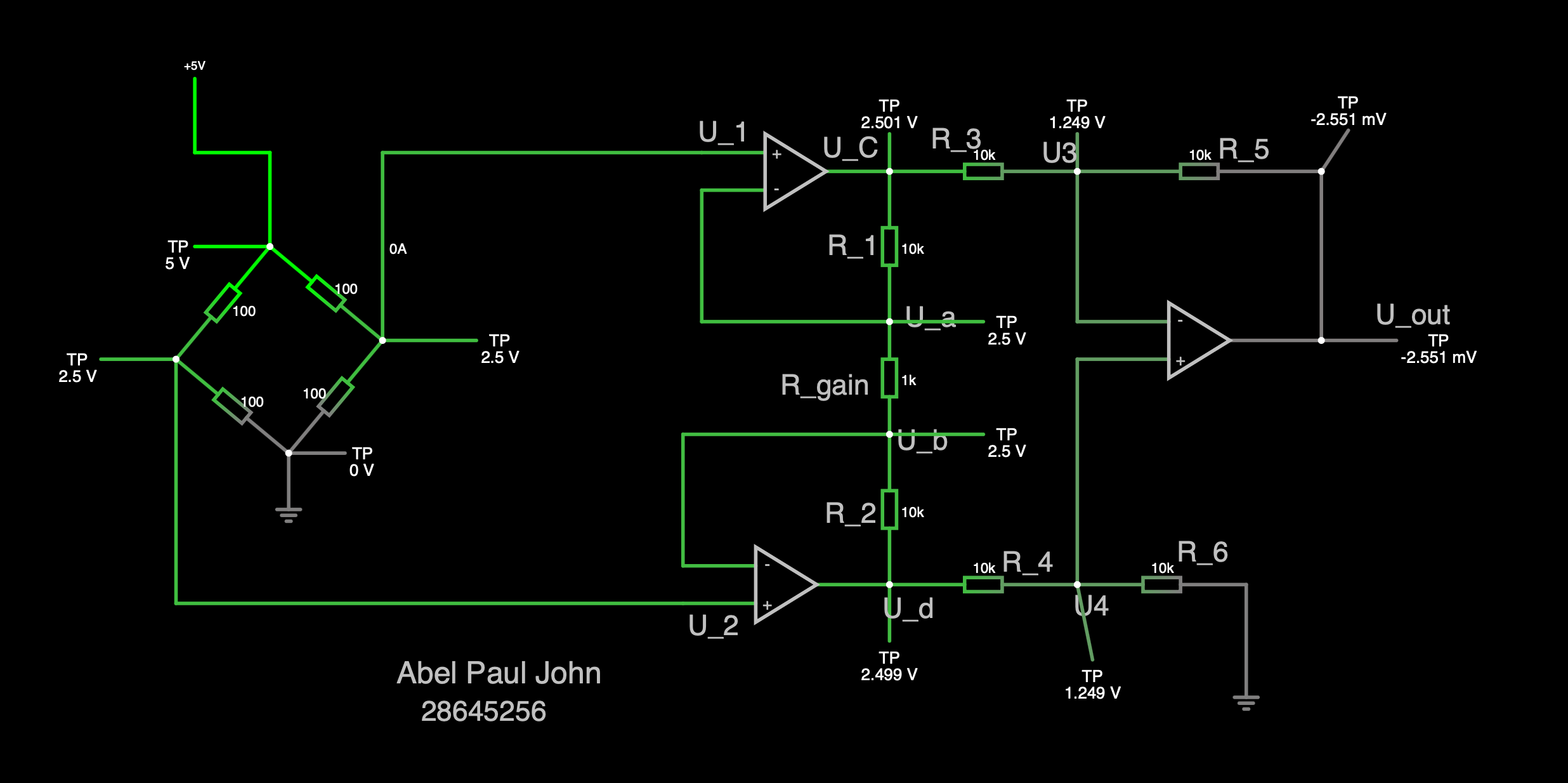
In the first circuit, I designed a balanced Wheatstone bridge powered by a 5V supply. The bridge contains four 100Ω resistors. Because all resistors have the same value, the bridge is perfectly balanced.
In this condition, both middle nodes of the bridge have a voltage of approximately 2.5V. This means there is no voltage difference between them. I connected these nodes to a multi-stage operational amplifier circuit.
Since the input voltages are equal, the differential voltage is zero. The output of the amplifier is therefore very close to 0V, which is confirmed in the simulation results.
This shows that the circuit works correctly. The amplifier does not produce a false signal when the bridge is balanced. This type of circuit is commonly used in sensor systems such as load cells and strain gauges, where very small voltage changes must be detected accurately.
Through this design, I demonstrated that I understand bridge circuits, symmetry in resistor networks, and differential amplification.
2. Weighted Operational Amplifier Circuit
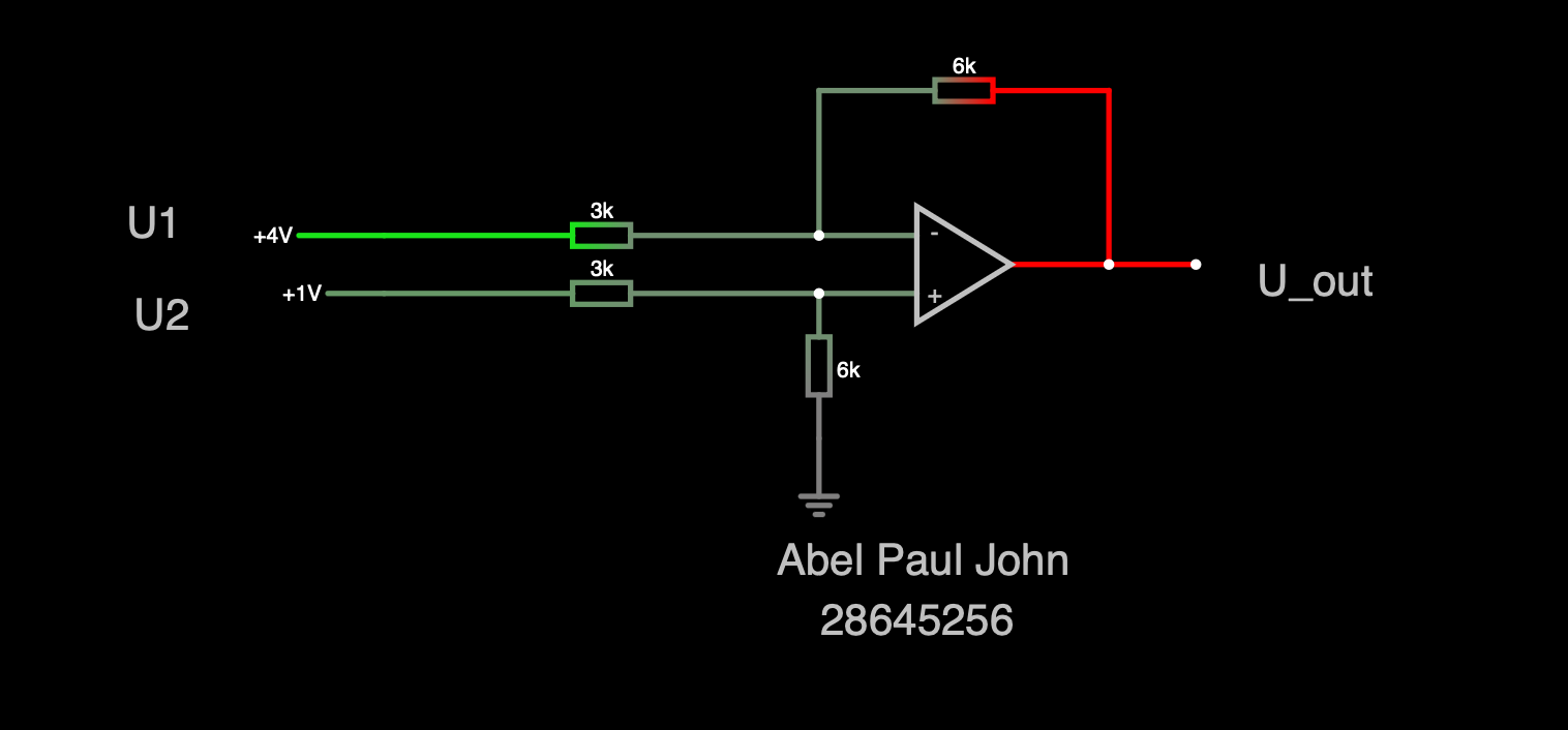
In the second circuit, I analyzed an operational amplifier with two different input voltages. The first input voltage is 4V and the second input voltage is 1V. The input resistors are 3kΩ and the feedback resistor is 6kΩ.
Using the resistor ratio, the gain of the amplifier can be calculated. The gain is equal to the feedback resistor divided by the input resistor. In this case:
Gain = 6kΩ / 3kΩ = 2
This means the amplifier scales the input signal by a factor of two. The simulation shows that the output voltage behaves exactly as predicted by theory. The circuit also follows the virtual short principle of operational amplifiers, meaning the voltage difference between the positive and negative input is almost zero.
This circuit demonstrates my understanding of operational amplifier theory, gain calculation, feedback networks, and signal scaling. Such circuits are often used in signal processing, audio systems, and sensor interfaces.
3. Voltage Divider and Amplification Stage

In the third circuit, I built a resistor ladder network connected to an operational amplifier. The goal was to analyze how current flows through different branches and how the output voltage is affected.
The simulation shows different current values in each branch. For example, one branch carries around 23.9 mA, while another branch carries 2.4 mA. The operational amplifier input current is very small, which matches the theory of an ideal op-amp.
The output voltage of this circuit is approximately 1.364V. This value matches the calculated result based on the resistor ratios and input voltages.
This part of the project helped me better understand current distribution, node voltage analysis, and amplifier biasing.
Engineering Approach
In this project, I followed a structured engineering process:
- Mathematical Modeling: Calculated the expected voltages and gains using pure theory.
- Virtual Prototyping: Built the circuits in simulation using Falstad.
- Verification: Checked every important node voltage and current value.
- Validation: Compared the simulation results directly with my theoretical calculations.
All circuits behaved exactly as expected. This confirms that the design is correct and stable.
What This Project Shows
This project demonstrates that I understand important concepts in precision analog electronics, including:
- Wheatstone bridge circuits
- Differential voltage measurement
- Operational amplifier gain and Feedback networks
- Current flow and node analysis
- Biasing and signal stability
More importantly, it shows that I strictly use simulation as a professional tool before moving to hardware implementation. This risk-mitigation mindset completely reduces mistakes and improves efficiency in real-world hardware projects.
Conclusion
Through this project, I strengthened my understanding of precision analog circuit design. I learned how small voltage differences can be amplified correctly and how resistor networks control gain and stability.
These fundamental skills are very important in embedded systems, sensor technology, and measurement systems boundaries. This project deeply reflects my engineering philosophy: combining theory, simulation, and practical design in a structured and professional way.
End of Case Study.
View all projects